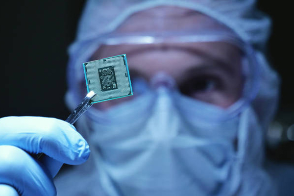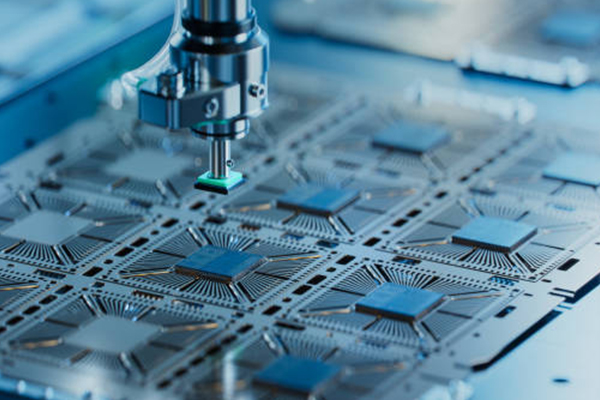
Ozone in Semiconductor Manufacturing
Ozone serves as a critical processing material in semiconductor manufacturing, enabling multiple high-precision steps through its strong oxidation capability and low-temperature reaction characteristics. Its applications span across cleaning, thin film deposition, surface treatment, and contamination control.
Core Applications
Surface Cleaning & Preparation
Removes organic contaminants, metal impurities and photoresist residues from wafers. Modifies surface properties to enhance adhesion and improve hydrophilicity. Performs precise etching of metal oxides including TiO₂ and ZnO.
Thin Film Processes
Grows high-quality silicon dioxide (SiO₂) layers at low temperatures. Serves as oxidizer in ALD and CVD processes for high-k dielectrics. Forms dense passivation layers (SiOx, SiNx) for device protection.
Process & Environmental Control
Efficiently strips photoresist through low-temperature ashing. Treats exhaust gases by decomposing VOCs and hazardous emissions. Supports TEOS-based deposition and dry cleaning applications.
Technical Advantages
Operates effectively at low temperatures
Leaves no chemical residues
Enables precise process control
Reduces environmental impact
Compatible with thermal-sensitive materials
Ozone has become indispensable in advanced semiconductor manufacturing, particularly for processes requiring high purity, precise material control, and environmental sustainability.